Impedance Control In PCB Design
Understanding Controlled Impedance in PCB Design
 What is Controlled Impedance in PCBs? Controlled impedance refers to the specific resistance that an electrical signal encounters as it travels along a PCB trace. This impedance is a combination of resistance, capacitive reactance, and inductive reactance. It’s a critical parameter in defining the performance of electronic circuits, components, and materials, particularly for high-frequency signal transmission. In simpler terms, controlled impedance ensures that signals are transmitted with minimal distortion, preserving signal integrity.
Why is Controlled Impedance Essential in PCBs? As electronic devices evolve, the demand for precise signal transmission has increased, making controlled impedance a vital aspect of modern PCB design, especially in communication technologies. Here’s why:
- Higher Operating Frequencies: The continuous rise in the operating frequencies of electronic devices necessitates strict impedance control to maintain signal integrity.
- High-Fidelity Signal Transmission: Controlled impedance ensures that signals are transmitted accurately, without loss or distortion, which is crucial for high-fidelity applications.
- Advancements in IC and SMT Technology: The development of more sophisticated integrated circuits and surface-mount technologies has made controlled impedance indispensable in PCB manufacturing.
- Embedded Components: As more components are embedded within PCBs, managing impedance becomes critical to avoid signal degradation.
- Enhanced Circuit Performance: Proper impedance control helps circuits resist interference, reduce crosstalk, and maintain stability, ensuring the reliability of electronic systems.
Request Your Free Quote Today!
Theoretical Foundation of Controlled Impedance
Understanding the Theory Behind Controlled Impedance
In transmission line theory, factors such as resistance, inductance, leakage conductance (the inverse of leakage resistance), and distributed capacitance relative to the reference layer (reference plane) significantly impact signal transmission speed and energy. These elements collectively influence how a signal propagates along a wire, affecting its speed and integrity. The signal level at any point on a transmission line depends not only on time but also on the distance along the line, with variations in current at different points.
For PCB traces, where the line width is consistent and the medium and thickness between the trace and the reference layer are uniform, the PCB trace can be treated as a uniform transmission line. This concept is illustrated by considering the trace as a series of small, unit-length transmission lines, each contributing to the overall impedance characteristics. This approach allows us to model and analyze the impedance using an equivalent circuit, ensuring that the PCB design meets the necessary performance requirements for high-speed signal transmission.
Classification of Controlled Impedance
Types of Controlled Impedance
Controlled impedance can be categorized based on the number of traces and transmission methods, as well as the mode of transmission:
By Trace and Transmission Method:

- Single-ended Impedance: Consists of a single trace plus a ground layer.
- Differential Impedance: Consists of two traces plus a ground layer.
 By Transmission Mode:
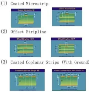
- Microstrip Line: An impedance line with one side parallel to the ground layer, separated by a dielectric, with the other side covered by a solder mask or left uncovered.
- Stripline: An impedance line that is sandwiched between two ground layers, offering better signal isolation compared to microstrip lines.
Common Types of Controlled Impedance in PCBs
While there are over 90 types of impedance in commonly used impedance calculation software like Polar-Si8000, the most frequently used types include:
- Surface Microstrip
- Offset Stripline
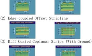
- Edge-Coupled Surface Microstrip
- Edge-Coupled Offset Stripline
Key Factors Affecting Impedance
Several factors influence the impedance values in a PCB, which should be considered during design:
- Dielectric Thickness: The thicker the dielectric, the higher the impedance (Z0).
- Conductor Trace Width/Space: Wider traces result in lower impedance (Z0).
- Dielectric Constant (Er): A higher dielectric constant reduces impedance (Z0).
- Conductor Thickness:
 Thicker conductors lower the impedance (Z0).
 - Solder Mask Thickness: Thicker solder masks slightly reduce impedance (Z0).
Impact of Factors on Impedance:
- Dielectric Thickness: 48% impact
- Conductor Width/Space: 24% impact
- Dielectric Constant (Er): 16% impact
- Copper Conductor Thickness: 8% impact
- Solder Mask Thickness: 4% impact
Understanding these factors is crucial for achieving the desired impedance in PCB designs, ensuring optimal performance for high-frequency signal transmission.
Impact of Dielectric Thickness
The thickness of the dielectric layer plays a crucial role in determining the impedance of a PCB. Different materials have varying compositions and thicknesses after pressing, which are influenced by the flatness of the press and the lamination process.
For any material used, it’s essential to know the achievable dielectric thickness to aid in design and calculation. As dielectric thickness increases, so does the impedance value. To maintain precise impedance, the thickness deviation should be controlled within at least 10%.
Influence of Dielectric Constant (Er/Dk)
The dielectric constant (Er) varies among different PCB materials:
- FR4: Dielectric constant ranges from 3.8 to 4.7.
- PTFE: Dielectric constant ranges from 2.9 to 3.9.
Impedance increases as the dielectric constant decreases. Therefore, materials with a lower dielectric constant are preferred when higher impedance values are required for optimal signal transmission.
Impact of Conductor Thickness
The thickness of the copper conductor directly affects the impedance:
- Thicker Copper: Results in lower impedance.
- Thinner Copper: Should be used to achieve higher impedance values.
Uniform control of copper thickness is crucial. To balance the current and prevent uneven copper thickness, additional copper planes are often added. Additionally, for PCBs with uneven copper distribution on the top and bottom layers, cross and reverse PCB paneling may be necessary to ensure uniform copper thickness across layers.
Effect of Solder Mask Thickness
Applying a solder mask on the PCB reduces impedance:
- Single Application: Typically reduces single-ended impedance by 2 Ohms and differential impedance by 8 Ohms.
- Multiple Applications: The reduction doubles with each additional layer up to two, after which further applications have little to no effect.
Understanding and controlling these factors is essential for achieving the desired impedance values in PCB design, ensuring the board meets its performance requirements.
Optimizing Impedance Matching in PCB Manufacturing
Before production begins, PCB manufacturing engineers carefully review the Gerber files to ensure that the material and stack-up are optimized for the required impedance. Here’s how our engineers achieve controlled impedance matching:
 Dielectric Thickness and Stack-Up Optimization
Adjusting the dielectric thickness is crucial for achieving the desired impedance:
- Increasing Dielectric Thickness: Raises the impedance value.
- Decreasing Dielectric Thickness: Lowers the impedance value.
Careful engineering design, precise lamination control, and tight material tolerances are essential to maintain the correct dielectric thickness.
Conductor Width and Spacing Adjustments
The width and spacing of conductors significantly impact impedance:
- Wider Conductor: Reduces impedance.
- Narrower Conductor: Increases impedance.
These dimensions are primarily controlled through meticulous etching processes and thoughtful design considerations.
Conductor Thickness Management
Conductor thickness also plays a vital role in impedance control:
- Thicker Conductor: Lowers the impedance.
- Thinner Conductor: Increases the impedance.
Conductor thickness can be managed through graphic electroplating or by selecting the appropriate base material with the desired copper foil thickness.
Solder Mask Application
The application of a solder mask can further fine-tune impedance:
- Single Application: Typically reduces impedance by 2 Ohms for single-ended impedance and 8 Ohms for differential impedance.
- Multiple Applications: Further reduce impedance proportionally with each additional layer, up to two applications. Additional layers beyond this may not significantly affect impedance.
By leveraging these techniques, our engineers ensure that the final product meets the specified impedance requirements, leading to optimal performance in your PCB designs.
How to Test Impedance in PCBs
When producing PCBs with controlled impedance, it’s crucial to ensure the impedance values align with customer specifications. Here’s how we test impedance before shipping:
 Impedance Testing Principle
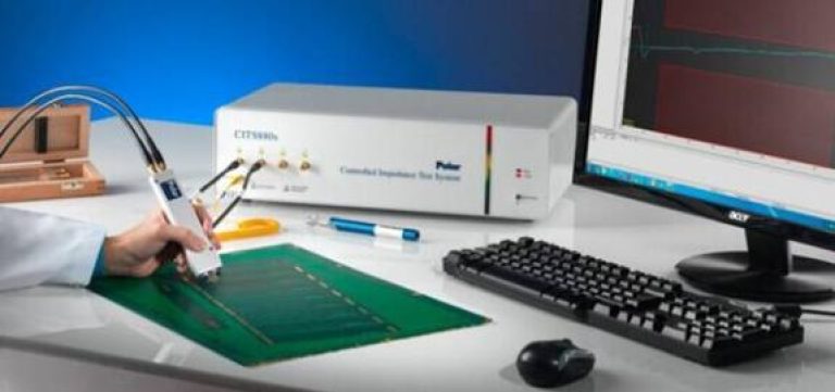
Impedance testing involves sending a pulse wave from an oscilloscope and analyzing the reflected wave. By comparing the transmitted and reflected waves, we can determine the impedance value based on the energy transmitted through the PCB.
Adding Impedance Coupons
To accurately test impedance, we include an impedance coupon on each PCB panel. This coupon features the same impedance lines and traces as the actual PCB and is manufactured under identical process conditions. If the impedance value on the test coupon meets the required specifications, we can confidently ensure the impedance on the finished PCBs is also within the desired range.
Using TDR (Time Domain Reflectometer)
We utilize a Time Domain Reflectometer (TDR), a specialized oscilloscope that generates pulse waves, receives them, and analyzes the results. The TDR allows us to accurately measure and confirm the impedance values of the PCBs.
Get Your Free Instant Quote Today!
Leap Electronic is your trusted partner and one-stop shop for PCB fabrication, component sourcing, PCB assembly, and electronic manufacturing. With over 16 years of expertise, we proudly serve over 1000 customers worldwide, delivering top-quality PCBs at competitive prices. Our ISO9001:2015 certification and UL listing ensure that all our products meet the highest industry standards. Every PCB is 100% E-tested and inspected using AOI and X-RAY, guaranteeing unparalleled reliability and performance.
Don’t wait – get an instant quote from our sales team today and experience the Leap Electronic difference. We’ll handle the rest!
