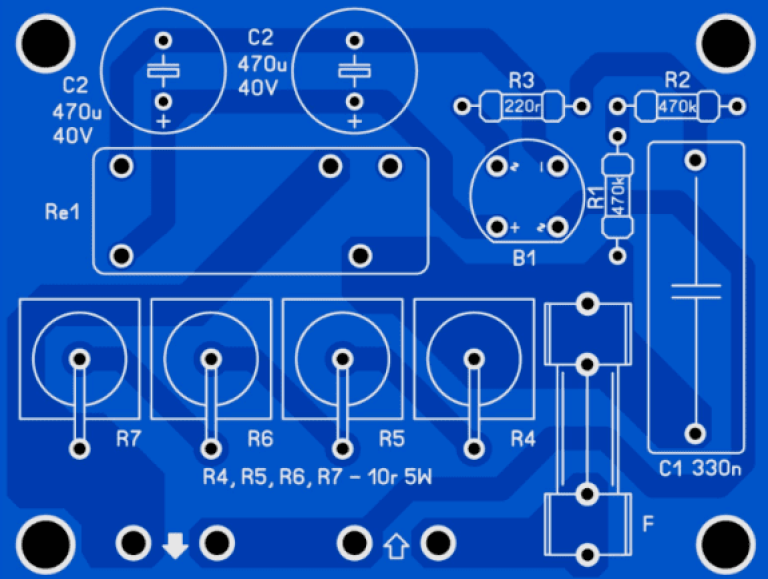
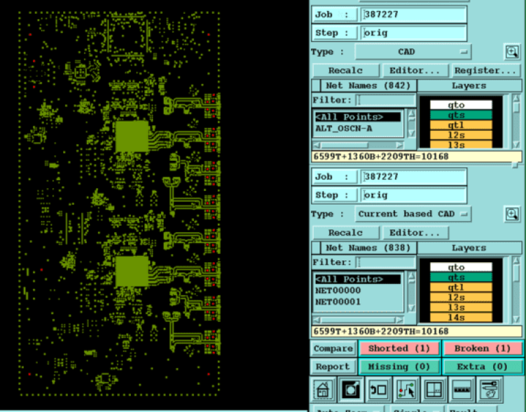
Complimentary PCBA File Review

Importance of DFM in PCB Production

Design for Manufacturing (DFM) is crucial in PCB production for several reasons:

  1. Error Detection: Errors can occur during the design phase or when converting PCB files between formats. Our engineers can identify and correct these issues before production begins, preventing costly mistakes.

  2. Material and Technology Compatibility: Not all materials or technologies specified in a PCB design are always available or suitable for manufacturing. We ensure that your design aligns with the capabilities of our manufacturing process, recommending alternatives if necessary.

  3. Optimization for Cost and Performance: We can enhance the robustness and cost-effectiveness of your PCB by optimizing aspects such as stack-up, material selection, and design parameters.

DFM Checks at LEAPPCB

At LEAPPCB, our experienced engineers conduct thorough reviews of your design files, including Gerber files and additional notes. Our DFM process focuses on key aspects to ensure your PCB is manufactured to the highest standards. Here are the primary elements we review during DFM:

  • File Consistency: Verifying the accuracy of the design files.
  • Material Compatibility: Ensuring the materials specified are available and suitable for the intended application.
  • Stack-Up Review: Assessing the layer structure for optimal performance.
  • Design Optimization: Identifying opportunities to improve the design for cost-efficiency and manufacturability.

Our goal is to ensure your PCB design is ready for seamless production, resulting in a reliable and high-quality final product.

Request Your Free Quote Today!

Material Selection and Optimization

In some instances, material changes are necessary due to factors such as extended lead times or the discontinuation of a specific material type or thickness. When this occurs, we will recommend an appropriate substitute and seek your approval to ensure the change aligns with your project’s requirements.

To optimize costs and maximize material utilization, we employ advanced software to determine the most efficient array style and size. This approach typically achieves a minimum of 85% utilization for single or double-sided boards and at least 75% for multi-layer boards. This careful planning ensures that we deliver cost-effective solutions without compromising on quality or performance.
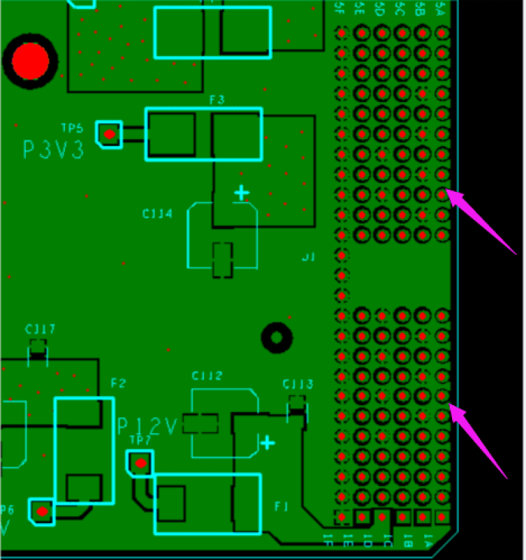
Tolerance We carefully review the hole sizes and tolerances to ensure they are within a reasonable range, except where specific requirements are provided by the customer. Some unique holes, like press-fit holes, require precise tolerances. For improved assembly, we maintain a maximum tolerance of 2 mil for press-fit holes.

Vias

  • Small Vias: Small vias can be challenging to clean, leading to solder mask ink residue. We recommend using plug holes to prevent this issue. If the vias are too large, reducing their size can improve the plugging effect.
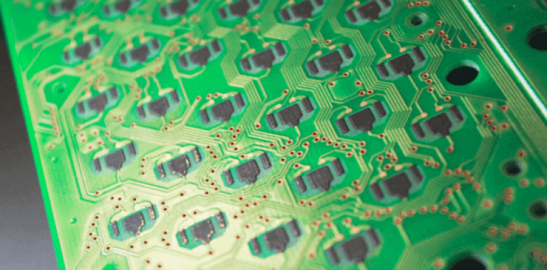
  • BGA Position: For vias around BGA positions, we recommend using plug holes to prevent tin beads from entering the vias during SMT, reducing the risk of shorts and open circuits.
  • SMT Pad Proximity: Vias that are too close to SMT pads should be moved to prevent potential issues. To reduce costs, we can manually optimize and reposition pads over vias. If position movement isn’t possible, we opt for resin plug holes with electroplated hole filling.
  • Flexible Boards: For flexible PCBs, through-holes in the flexible area are relocated to the reinforcement or rigid board area to extend the board’s service life. We also match the copper thickness in the flexible area to improve the board’s bending properties, based on the usage habits of the customer’s product

Buried-Blind Holes In multi-layer boards, buried-blind holes are essential for achieving high-density interconnections. By appropriately adjusting the dielectric thickness of each layer, we can use advanced layer interconnection techniques to effectively implement all types of buried-blind holes.

Back Drilling

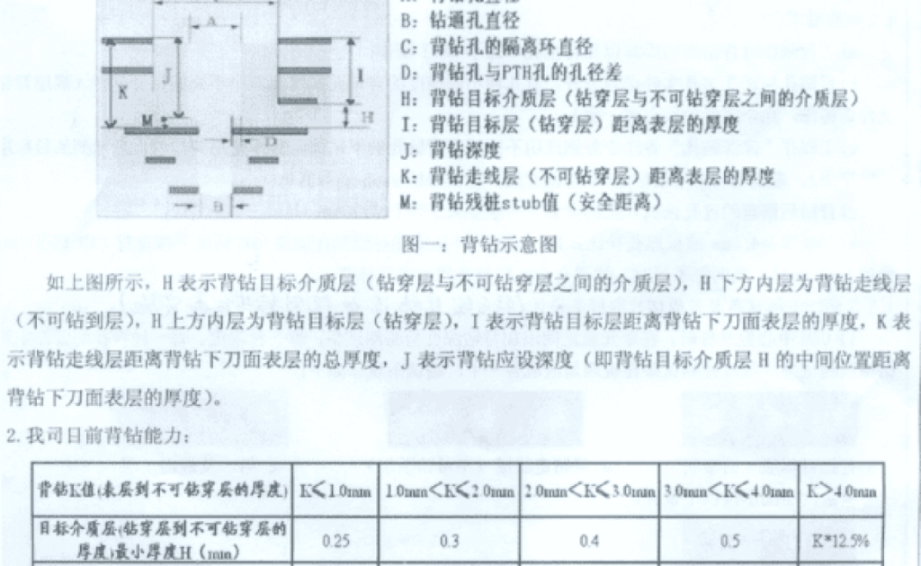
Back drilling is an effective technique to reduce costs and simplify technical challenges. Its primary function is to remove the unnecessary portions of through-holes in the PCB that do not contribute to connection or signal transmission. This prevents issues like reflection, scattering, and delay in high-speed signal transmission. Below are our capabilities for back drilling:

  • Precision: Our back drilling process ensures minimal impact on signal integrity, offering a clean and efficient solution for high-speed applications.
  • Versatility: We can accommodate various designs and requirements, tailoring the back drilling process to meet the specific needs of your PCB.
Depth-Controlled Routing

Depth-controlled routing allows for precise control over the depth of drilled holes, ensuring they meet specific design requirements. This technique is essential for creating complex, multi-layer boards with varying depths, ensuring each layer functions as intended.

Copper Plating

To ensure consistent and high-quality electroplating across the entire PCB, we implement several key processes:

  • Uniform Electroplating: We enhance the uniformity of electroplating by adding an auxiliary copper sheet around the working board during the electroplating process. This technique helps achieve a more even distribution of copper across all areas of the board.

  • Real-Time Monitoring: Our electroplating solutions are closely monitored with advanced data systems, allowing for timely detection and adjustments. This ensures that the copper plating process remains within optimal parameters throughout production.

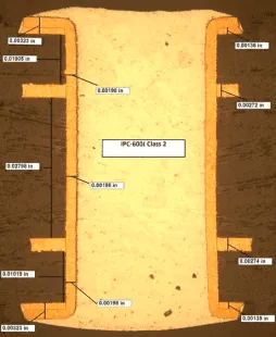
  • Precision Measurement: After electroplating, we meticulously measure the copper thickness on each layer of the PCB to ensure it falls within the specified tolerances. This careful attention to detail guarantees the reliability and performance of your finished product.

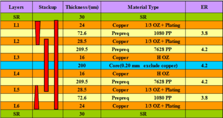
6 Layer stackup

our standard 1.0mm HDI 1+N+1 stack-up

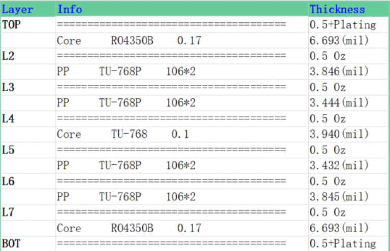
our quality department meticulously checks the thickness of each dielectric layer

BGA Solder Mask Opening
  • The recommended solder mask opening for BGA is BGA size + 4 mil.
BGA Layout Suggestions
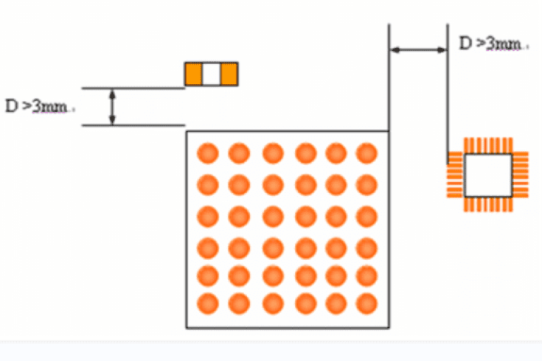
  • Component Placement: To facilitate easier BGA repair, avoid placing any components within a 3mm radius around the BGA.
  • Power Supply Optimization: To enhance the BGA power supply’s filtering and energy storage, it is advisable to place capacitors greater than 22uF around the BGA.
Small BGA Pads
  • For very small BGA pads around 0.2mm, it can be challenging to control their size and shape during the etching process. To address this, we recommend using the solder mask defined pads technique, where the solder mask opening is slightly smaller than the corresponding copper pads. This approach helps maintain precision and reliability in the BGA layout.

Impedance Simulation

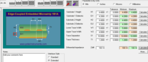
To ensure accurate impedance control, we use advanced Polar software to analyze and simulate impedance values, providing detailed insights as shown below:

Additionally, we generate a comprehensive impedance analysis report, similar to the example provided below, to ensure that all parameters meet the specified requirements. This thorough approach guarantees the integrity and performance of high-speed signal transmission in your PCB designs.

Panelization in PCB Manufacturing

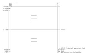
Often, customers provide files for single PCBs, but we frequently recommend suitable panelization to streamline both PCB manufacturing and assembly processes. Two common panel types are those with V-cuts and those with mouse bites. Below, we outline the advantages and disadvantages of each:

V-Score Design Adjustments to Meet Customer Needs:

  • 30° V-Score: The distance between the copper and the V-score centerline should be > 0.35mm to avoid exposing copper at the board’s edge.
  • 45° V-Score: The distance between the copper and the V-score centerline should be > 0.4mm to prevent copper exposure at the board’s edge.
  • Board Thickness ≤ 0.40mm: We recommend single-sided V-CUT with a residual thickness of 0.20 ± 0.10mm. The copper distance to the V-score centerline should be > 0.4mm to avoid exposing copper.
  • Board Thickness > 1.0mm and < 1.6mm: The residual thickness should be 0.4 ± 0.1mm.
  • Board Thickness > 1.60mm: The residual thickness should be 0.5 ± 0.1mm.
  • Edge Finishing: We advise rounding all sharp edges to prevent puncturing packaging during handling.

This attention to detail in panel design ensures the integrity of the PCB throughout manufacturing and assembly, while also accommodating customer-specific requirements.

Optimized Guidelines for Drill and Solder Mask Design

1. Drill Design

  • Isolation Clearance for NPTH:

    • Ensure that the isolation clearance between the Non-Plated Through Hole (NPTH) and the outer copper is generally ≥ 0.20mm, with a minimum clearance of ≥ 0.15mm. This increase in the minimum gap helps prevent issues like the silk screen line’s solder mask from turning red.
  • Second Drill Copper Digging:

    • For second drilling after etching, the copper cut in the center should be 0.10mm smaller on one side of the hole.
    • If the second drilling occurs before routing, the minimum distance from the edge of the second drill to the copper or trace edge should be 0.10mm.
    • Ensure that the annular ring after the second drill is at least 0.3mm on one side, particularly for second-drilled rings based on 2oz copper.

2. Solder Mask Design

  • Pad Clearance:

    • Check the solder mask Gerber file to ensure there is no solder mask on the pads. The solder mask should be exposed as much as possible to minimize substrate leakage, with the opening size being one mil larger than the pad on each side.
  • Solder Mask Dam at Golden Fingers:

    • If the solder mask dam is at the golden finger, it is advisable to delete it and expose both ends of the slot if the current design is unreasonable.
  • BGA Pad Definition:

    • For BGAs that are too small, leading to poor etching control, it is recommended to change the BGA size and opt for solder mask-defined pads to ensure better precision.
  • Via Plugging Around BGA:

    • Vias around the BGA should be plugged with solder mask ink to reduce the risk of open-short circuits.
  • Solder Mask Design for PTH and NPTH:

    • Implement a thorough review of the solder mask design for both Plated Through Holes (PTH) and Non-Plated Through Holes (NPTH) to ensure optimal performance and reliability.

By following these optimized drill and solder mask design guidelines, you can enhance the manufacturing process, improve yield rates, and ensure high-quality PCB production.

Optimized Solder Mask Design Guidelines for PTH and NPTH

Solder Mask Design for PTH (Plated Through Holes)

  • General Clearance:

    • Always check the solder mask Gerber file to ensure no solder mask overlaps with the pads.
  • Small Hole Consideration:

    • For holes with a diameter less than or equal to 0.5mm, ensure they are not blocked by the solder mask.
  • Larger Holes:

    • If the hole opening is larger than the hole itself but smaller than the pad, and solder mask ink is not permitted to enter the hole, the solder mask blocking light point should be 0.1mm larger than the hole diameter.

Solder Mask Design for NPTH (Non-Plated Through Holes)

  • Larger Diameter Holes:

    • For NPTH with a hole diameter of ≥ 0.6mm, the solder mask blocking light point should be made 0.05mm smaller than the single side of the hole diameter.
  • Smaller Diameter Holes:

    • For NPTH with a hole diameter of less than 0.6mm, the solder mask blocking light point should be made 0.05mm larger than one side of the hole diameter.
  • Plugging Holes:

    • Cancel the solder mask blocking light point for holes that require plugging.

Key Principles for Solder Mask Application

  • Maintaining Design Integrity:

    • Do not alter the position of the original solder mask exposure area or the reserved solder mask area. It is crucial to retain the original design’s solder bridge, except when the bridge is too small to be maintained.
  • Critical Factors:

    • The two essential factors in solder mask design are the window size and the distance from the window to the nearest line.

Solder Mask Opening Adjustments Based on Copper Thickness

  • Copper Thickness Considerations:

    • For copper thicknesses less than 1oz, the solder mask (S/M) opening should be 0.05mm larger than the pad on one side of the line pad, typically made with a 0.08mm edge. If this leads to exposed lines or the inability to retain the minimum solder mask dam, reduce the S/M opening to at least 0.03mm.
    • For 1oz ≤ base copper <2oz, the S/M exposure is 0.05mm larger than one side of the compensated line or pads.
    • For 2oz ≤ base copper <3oz, the S/M exposure is 0.03mm larger than one side of the compensated line or pad.
    • For 3oz ≤ base copper <4oz, the S/M exposure is 0.02mm larger than one side of the compensated line or pad.
    • For base copper ≥ 4oz, the S/M exposure is 0.01mm larger than one side of the compensated line or pad.
  • BGA Openings:

    • For BGA solder mask openings, the minimum S/M exposure should be 0.03mm larger than one side of the compensated line or pad to ensure proper exposure and avoid potential issues during the process.

These optimized guidelines ensure the integrity of the solder mask design, enhance manufacturing quality, and prevent potential issues during PCB production.

Carbon Design

  • Printing Pad Size:

    • The printing pad should be at least 10 mil larger than the copper pad, with a minimum line thickness of 10 mil.
  • Spacing Considerations:

    • The minimum distance between printing pads should be 10 mil. For line pads, maintain a minimum spacing of 30 mil when there is green oil between the carbon oil fingers.
    • If there is no green oil between the carbon oil fingers, the spacing between printing pads should be 30 mil, and the line pad spacing should be at least 50 mil.
  • Carbon Oil Seepage:

    • To prevent carbon oil from seeping into the hole ring and other pads, ensure the minimum distance from the carbon oil film’s printing pad to the hole ring and other pads is 10 mil.

Silkscreen Design

  • Text Specifications:

    • Word Width: 5 mil for the base material surface, 6 mil for the line surface.
    • Word Height: Minimum of 0.8 mm.
    • Minimum Word Gap: 6 mil.
    • Minimum Character Spacing from Pads: 6 mil.
  • Character Orientation:

    • Ensure that characters on the bottom side are correctly mirrored to avoid errors that could affect readability. Adjust as necessary and inform the customer for future reference.
  • Character Clarity:

    • Adjust the line width of small characters to ensure they are clear and easy to recognize. Inform the customer of any adjustments for future designs.
  • SMT Process Preparation:

    • Identify and remove any characters on pads in preparation for the SMT process.
  • UL Logo and Date Code:

    • It is recommended to include the UL logo and date code on the silkscreen layer to protect customer interests and provide a reference for future traceability.
CAM Analysis and Optimization
  • Genesis2000 System:

    • Utilize the Genesis2000 system for data input, DFM (Design for Manufacturing) optimization, editing, analysis, and output. Ensure all customer files, especially network files, are transferred into Genesis for accurate network comparison and consistency verification.
  • Network Analysis:

    • Perform network analysis to identify potential open and short circuits, helping customers avoid future issues.
Copper Layer Design and Optimization
  • Annular Ring in Inner Layers:

    • If the hole ring is insufficient, compensate according to manufacturing requirements. The annular ring size should be:
      • 1 oz: ≥ 0.10mm
      • 2 oz: ≥ 0.13mm
      • 3 oz: ≥ 0.20mm
      • 4 oz: ≥ 0.30mm
  • Teardrop Design:

    • Use software detection functions to identify areas where teardrops are needed. Add teardrops to increase the connection reliability between PTH holes and inner layers, ensuring the minimum gap meets MI requirements.
  • Inner Functional Pad:

    • Ensure the number of connecting wires for inner functional pads is at least 2. The size of the isolation ring for inner functional pads should generally be 0.25mm, with the minimum isolation clearance not less than 0.12mm.
Additional Optimizations
  • Non-Functional Pads:

    • Remove all non-functional independent pads in the inner layers (except for blind and buried holes) to reduce the risk of internal short circuits.
  • Power Grabbing Copper Sheet:

    • When adding power grabbing copper sheets in the inner layer of the groove, make each corner a fillet (generally R ≥ 2mm) to facilitate the flow and exhaust of resin. Avoid right angles or acute angles.
  • Inner Layer Network Check:

    • Conduct a Net-list (network) check to ensure the electrical performance of the production line graphics is consistent with the raw data, reducing the risk of design issues during production.

These enhanced design and optimization guidelines ensure the highest quality and reliability in PCB manufacturing, meeting industry standards while addressing specific customer requirements.

Get Your Free Instant Quote Today!

Leap Electronic is your trusted partner and one-stop shop for PCB fabrication, component sourcing, PCB assembly, and electronic manufacturing. With over 16 years of expertise, we proudly serve over 1000 customers worldwide, delivering top-quality PCBs at competitive prices. Our ISO9001:2015 certification and UL listing ensure that all our products meet the highest industry standards. Every PCB is 100% E-tested and inspected using AOI and X-RAY, guaranteeing unparalleled reliability and performance.

Don’t wait – get an instant quote from our sales team today and experience the Leap Electronic difference. We’ll handle the rest!

China First 7-Day Delivery Headset Factory​, Free Samples Available.

Ask For A Quick Quote

We will contact you within 1 working day, please pay attention to the email with the suffix “@techpinn.com”