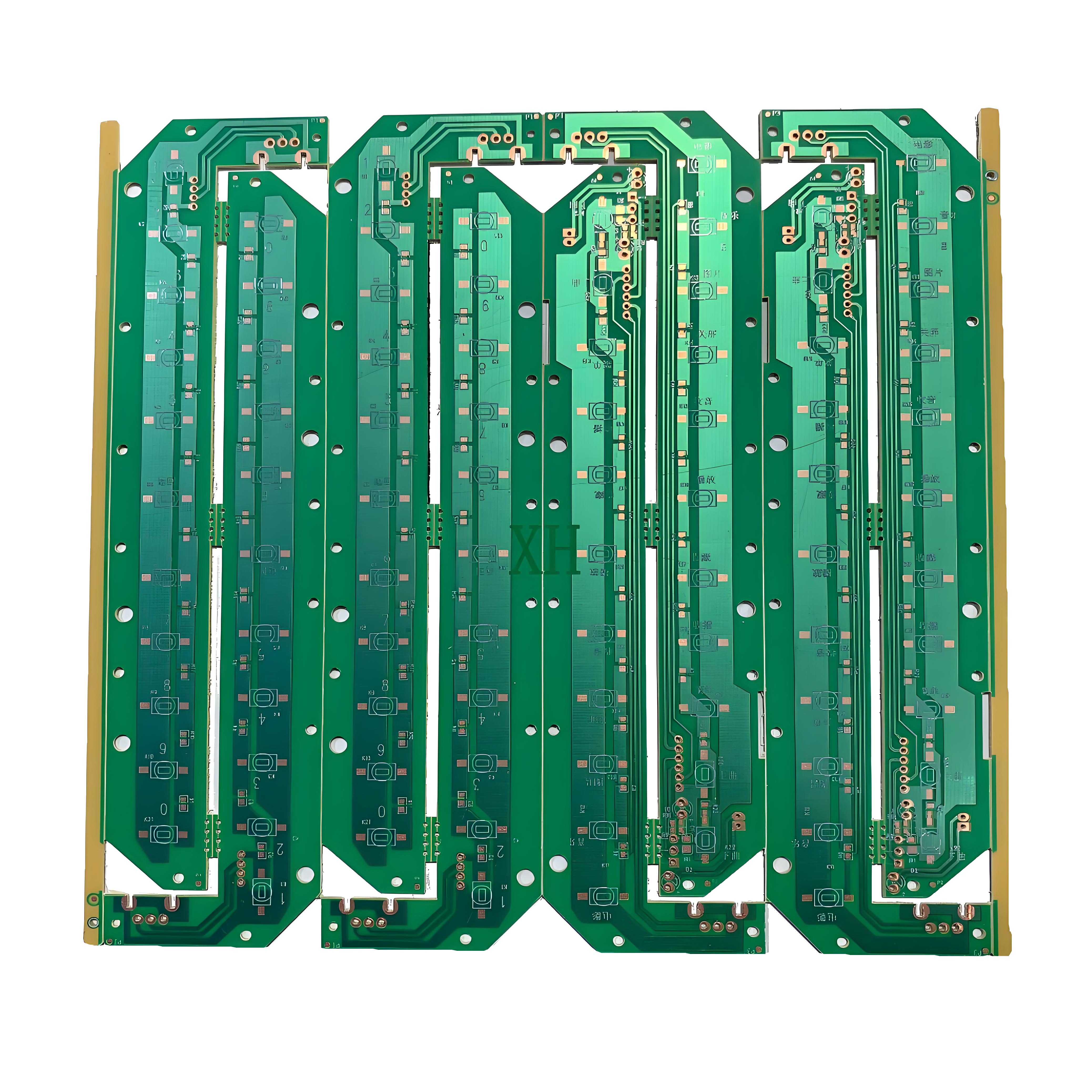
Steps in PCB Reverse Engineering
Sometimes, the necessary documentation for a custom PCB may be lost, yet a replica is required. In such cases, PCB Reverse Engineering, also known as PCB Copying, becomes essential. Here are the general steps to duplicate an existing PCB:
Obtain the Original PCB: Start with a physical copy of the original PCB. This could be acquired through purchase, borrowing from the original manufacturer, or creating a physical copy using a scanner or digital camera.
Design the PCB: Utilize PCB design software such as Altium Designer, Eagle PCB, or KiCAD to create a new design based on the original PCB. Use the existing PCB as a reference for component placement and trace routing.
Generate Gerber Files: Once the new PCB design is complete, generate Gerber files. These files contain all the necessary information for manufacturing the PCB and are the standard format used by PCB manufacturers.
Choose a PCB Manufacturer: Select a PCB manufacturer that meets your specifications and requirements. This decision is crucial, so take time to evaluate options carefully.
Submit the Gerber Files: Provide the Gerber files to your chosen PCB manufacturer. Ensure that all requirements are met and any additional specifications are clearly communicated.
Verify and Test the Copied PCB: After the PCB is manufactured, verify that it matches the original in terms of size, component placement, and routing. Perform thorough testing to ensure it functions as expected, using circuit testers or by installing it in the intended device.
Important Note: Copying a PCB without the original manufacturer’s permission may be illegal and can lead to legal consequences. Always ensure you have the appropriate rights to replicate the design.


