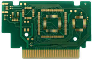
Multilayer PCBs
Top Prototype PCBs at Competitive Prices
Choose from a wide range of high-performance materials, including CEM1, CEM4, Standard FR4, High TG FR4, Halogen-Free FR4, High-Speed FR4, Polyimide (PI), PET, PTFE, Metal Core, Ceramic, and BT Laminate.
- Prototypes Up to 100 Layers: Perfect for complex designs.
- Advanced Via Technology: Blind & buried vias, micro vias, via plugging, and VIAPPO for optimized performance.
- Precision Engineering: Impedance control, heavy copper up to 40 oz, back drilling, backplanes, embedded devices, and IC substrates.
- Certified Quality: ISO 9001:2015 certified and UL listed, ensuring top-notch reliability and safety.
Printed circuit boards (PCBs) are the essential frameworks that electrically and physically connect a multitude of components within electronic devices. From simple single-layer designs to intricate multi-layer configurations, PCBs are vital to the functionality of modern technology. Turning a conceptual idea into a fully functional PCB requires a systematic approach, including thorough development, qualification, and pre-production testing. Skipping these critical steps and rushing into high-volume production can lead to significant failures and costly setbacks. Proper assessment and validation are key to ensuring reliable and successful PCB production.
Request Your Free Quote Today!
Understanding PCB Prototypes
A PCB prototype is an early sample of a printed circuit board created to test and validate the design before full-scale production. These prototypes are crucial for verifying that the board meets all specifications and performs as intended. Through rigorous testing, the prototype may undergo several design iterations to refine its functionality. Once the prototype is verified, small-scale preproduction can simulate its performance on a larger scale. The ultimate goal is to perfect the design, ensuring it meets predefined performance standards, quality, and cost-effectiveness before mass production.
Discover the Advantages of PCB Prototypes
Preventing Failures Early
During the prototyping phase, printed circuit boards (PCBs) undergo meticulous scrutiny by design, manufacturing, product, and test engineers. Early detection of potential issues is achieved through software simulations, defect analysis, and failure investigations. These assessments allow for enhancements in the design, reducing the likelihood of failures in the final product. Reliability tests are conducted to evaluate how materials degrade under conditions such as voltage, temperature, vibration, and humidity, ensuring long-term durability.
Minimizing Costly Returns
One of the key advantages of comprehensive PCB prototyping is the ability to identify and resolve design errors before mass production. By addressing issues during the prototyping stage, costly returns and customer complaints are significantly reduced. Design iterations and material revisions can be made swiftly, leading to a more refined product and minimizing the risk of expensive repairs and rectifications.
Optimizing Design for Performance and Cost
Prototyping provides the opportunity to refine and optimize the PCB design, allowing for improvements in both functionality and cost-effectiveness. As prototypes are built and tested, new ideas and enhancements often emerge, enabling the creation of a superior product that meets both performance and budgetary goals.
Defining Requirements More Accurately
Creating prototypes also helps to clarify and document project requirements that may have been overlooked in the initial stages. Testing prototypes reveals potential gaps in design, machine capabilities, and test requirements. These insights allow for adjustments and discussions with customers, ensuring that the final requirements are clearly defined and met.
Step-by-Step Guide to PCB board Prototypes
Key Steps in Developing and Manufacturing a PCB Prototype
1. Schematic Capture
The first step in creating a PCB prototype is generating a detailed schematic diagram using Electronic Design Automation (EDA) software. This schematic is the blueprint for the entire design, defining circuit connections and functionality. Components and connections are represented by symbols, providing a clear theoretical view of the circuit. During this stage, Design for Manufacturing (DFM) is also performed to ensure compatibility between the design and manufacturing processes. DFM helps eliminate costly design revisions later by simplifying the design and selecting the optimal materials, balancing cost and performance.
2. PCB Prototype Layout
Next, the schematic is transformed into a physical PCB layout, specifying the locations and connections of all components. This layout visualizes circuit tracks, grounding, and routing, while also defining critical dimensions like conductor and separation widths to prevent voltage spikes and operational issues. A design rule check (DRC) is conducted at this stage to ensure the layout adheres to all design limitations, resulting in a reliable and high-performance PCB prototype.
3. Board Fabrication
Once the layout is finalized, the Gerber file, containing all layer-specific information, is sent to the manufacturer. This file guides the fabrication process, which may include material cutting, drilling, through-hole plating, laminating, etching, solder masking, and solder-resist application. The exact steps vary depending on the design and number of layers, but each process is crucial to creating a precise and functional PCB prototype.
4. PCB Prototype Testing
After fabrication, the PCB prototype undergoes rigorous testing to ensure it meets all design specifications. A flying probe tester is typically used for small-scale testing, checking circuit continuity and other key factors. At this stage, it’s important to have a robust test plan in place, selecting the appropriate probes, equipment, connectors, and sockets to address any physical constraints or interferences. Early design considerations for test pads, vias, and connector footprints are critical to successful testing and eventual mass production.
Key Factors in Choosing PCB Prototyping Services
Fast Turnaround Time
When speed is critical, PCB prototyping services deliver quick and precise results. Fast delivery ensures that prototype PCBs are produced with high accuracy, paving the way for efficient large-scale production. By reducing lead times, you minimize the risk of defects, enhance productivity, and lower overall costs.
Comprehensive One-Stop Service
A one-stop PCB prototype service covers every stage, from initial design and component sourcing to final production. This approach guarantees the reliability of materials and the quality of the finished PCB. The expertise of your PCB prototype supplier plays a crucial role in ensuring seamless service and high-quality prototype boards.
Uncompromised Quality
Quality is paramount in PCB prototyping because the prototype serves as the blueprint for mass production. A high-quality PCB prototype ensures that subsequent production runs meet all relevant standards and specifications. Experienced manufacturers provide reliable, high-quality prototypes that set the stage for successful large-scale manufacturing.
Advanced Capabilities
PCB prototypes are essential for developing cutting-edge technologies like HDI, rigid, and flexible PCBs. These prototypes serve as valuable references for high-end PCB manufacturing, ensuring consistent performance and reliability in the final product.
Competitive Pricing
Effective PCB prototyping helps streamline mass production, resulting in competitive pricing for large-scale orders. By understanding the challenges and processes involved during prototyping, manufacturers can minimize material and labor costs, making the production process more efficient and cost-effective.
Flexible Quantities
PCB prototyping allows you to gauge the feasibility of mass production and determine production cycles. This flexibility ensures quality assurance, whether you’re producing in small or large quantities.
Excellent Customer Support
Prototyping services provide valuable insights into PCB fabrication, offering customers a smooth and informative manufacturing experience. Great customer service ensures that you receive the support and information needed for successful PCB production.
Why Choose LEAPPCB as Your PCB Prototypes Partner?
Unmatched Capabilities
LEAPPCB specializes in providing a comprehensive range of rigid PCB solutions, accommodating various materials, layer counts, copper thicknesses, surface finishes, and technologies. Whether you require a straightforward one-layer PCB or a complex 100-layer HDI PCB with intricate vias and fine lines, we have the expertise to fulfill all your needs.
Competitive Pricing
We offer competitive pricing with flexible options tailored to your requirements. Share your technical specifications with us, and we will promptly provide you with a detailed quotation.
Superior Quality
Quality is at the heart of everything we do at LEAPPCB. Our commitment to delivering high-quality rigid PCBs is unwavering, driven by a zero-defect mindset and a culture of continuous improvement. Our production processes adhere to stringent quality management standards, including ISO9001, ISO13485, and TS16949.
Exceptional Customer Service
At LEAPPCB, we believe that open communication and collaboration are the keys to a successful partnership. We treat our customers as partners, aligning our goals with yours to ensure your success. We prioritize your needs and requests, delivering on our commitments every time.
Fast and Reliable Delivery
We are known for our reliability in meeting delivery deadlines. LEAPPCB offers fast turnaround times and expedited options to ensure your projects stay on track. Our adherence to delivery commitments is a testament to our dedication to your success.
Choose LEAPPCB for your rigid PCB needs and experience unparalleled service, quality, and expertise. Contact us today to discuss your project requirements!
Get Your Free Instant Quote Today!
Leap Electronic is your trusted partner and one-stop shop for PCB fabrication, component sourcing, PCB assembly, and electronic manufacturing. With over 16 years of expertise, we proudly serve over 1000 customers worldwide, delivering top-quality PCBs at competitive prices. Our ISO9001:2015 certification and UL listing ensure that all our products meet the highest industry standards. Every PCB is 100% E-tested and inspected using AOI and X-RAY, guaranteeing unparalleled reliability and performance.
Don’t wait – get an instant quote from our sales team today and experience the Leap Electronic difference. We’ll handle the rest!
Everything you need to know about Multilayer PCBs
- Placing an order for a PCB prototype is easy! Simply send an email to sales@leappcb.com or reach out to our sales team directly. We’ll process your order promptly and ensure a seamless experience. Feel free to contact us with any questions or to start your order today – we’re here to help!
We prioritize speed and efficiency in our PCB prototype services. You can expect your PCB prototype order to be completed within one week or less, ensuring that your project moves forward without delay. Fast turnaround times help you stay on schedule and bring your designs to life quickly.
We offer a wide range of PCB prototype options to meet your specific needs, including:
- Rigid PCB
- Flexible PCB
- Rigid-Flex PCB
- Advanced Via Technology: Blind, buried, staggered, stacked vias, and via-in-pad (VIPPO)
- HDI PCBs: i+N+i structure, Any-Layer HDI
- Specialized PCBs: Aluminum base, copper base, RF Microwave, high-frequency, high-speed, impedance control, and extreme copper up to 20 oz
- Backplane and Back Drill PCBs
- PCBs with IC Substrate
Yes, at LEAPPCB, all our PCB prototypes are backed by a warranty and undergo 100% E-testing before shipping. This ensures that you receive high-quality, reliable boards with complete peace of mind.
- Absolutely! We proudly provide PCB prototyping services to customers across the globe, ensuring top-quality solutions no matter where you are.
Our expert engineers will thoroughly review your PCB or Gerber files to ensure your design is optimized for manufacturing. We’ll provide detailed feedback and recommendations to help you achieve the best possible results.
- We gladly accept PCB files or Gerber files as our preferred formats. However, we’re also flexible and can work with other PCB file formats to meet your needs.
- Absolutely! You can request a sample of your PCB prototype before placing a full order. Simply reach out to our sales team, and they’ll provide you with all the details. We’re here to accommodate your needs, so don’t hesitate to contact us!
For PCB bare board prototypes, no components are needed as the focus is solely on the board’s fabrication. However, in PCB assembly prototypes, we utilize a wide range of components, including resistors, capacitors, IC chips, connectors, and more, to fully assemble and test your design.
At LEAPPCB, we make payments easy and flexible by accepting a variety of methods, including:
- Wire Transfer: Directly to our bank account.
- PayPal: Secure and convenient online payments.
- Payoneer: A reliable option for global transactions.
- Westunion: Fast and accessible for international payments.
- Aliexpress/Alipay: Trusted platforms for quick and easy transactions.
