PCB Produciton

Custom PCBs at Competitive Prices

Rigid, Flex, Rigid-Flex, HDI, Metal Core, Microwave & RF
1-40 Layer Mass Production & 100 Layer Prototypes
Advanced Features: Blind & Buried Vias, Micro Vias, Via Plugging, VIAPPO
Precision Engineering: Impedance Control, Heavy Copper up to 20 oz
Specialized Options: Back Drilling, Backplane, Embedded Devices, IC Substrates
Versatile Finishes: HAL, Immersion Gold/Silver/Tin, OSP, ENIG, ENEPIG, Soft Gold, Hard Gold Plating

Understanding PCB Production                            

Printed Circuit Boards (PCBs) are the backbone of every electronic device, typically seen as green, white, or black circuit boards. PCBs serve as the foundation for various electronic components, connecting them through intricate copper pathways embedded within the board.

In a narrow sense, PCB production refers to the manufacturing process of these circuit boards. However, the production of PCBs encompasses a wide range of expertise within the industry, including the history of PCBs, key terminology, types of base laminates used, detailed manufacturing processes, PCB acceptance standards, classifications, cost considerations, and insights into the current and future landscape of PCB manufacturing.

At LEAPPCB, we are committed to sharing this valuable knowledge with you. With over 16 years of experience, we specialize in small to medium-volume professional PCB manufacturing. Our China-based factory is UL-listed (E358677) and certified to ISO9001 and ISO13485 standards, ensuring top-quality production and reliability.

Request Your Free Quote Today!

Explore Our Advanced PCB Manufacturing Capabilities

At LEAPPCB, we offer a wide range of PCB manufacturing services to meet your most demanding project requirements. Our capabilities include:

  • Rigid PCBs: Durable and reliable for various applications.
  • Flexible PCBs: Ideal for designs that require bending and flexing.
  • Rigid-Flexible PCBs: Combining the best of both rigid and flexible boards.
  • Advanced Via Technologies: Including blind vias, buried vias, staggered vias, stacked vias, and Via in Pad (VIPPO) with options like S/M, epoxy, and copper plugging.
  • High-Density Interconnect (HDI): i+N+i structures, Any-Layer HDI, and more.
  • Specialty Materials: We work with FR4, polyimide, ceramic, alumina, PTFE, and more.
  • Metal-Based PCBs: Including aluminum and copper base PCBs for high-performance applications.
  • RF and Microwave PCBs: Designed for high-frequency and high-speed applications with precise impedance control.
  • Extreme Copper PCBs: Supporting copper thicknesses up to 20 oz for high-power designs.
  • IC Substrate PCBs: Offering specialized solutions for integrated circuits.
  • Backplane and Back Drill PCBs: For complex, high-layer count designs.

Material Types We Use:

  • High TG FR4, Halogen-Free FR4, High-Speed FR4
  • Polyimide (PI), PET, Semi-Flex Materials
  • Aluminum, Copper, Alumina Ceramic, Special Alloys
  • High-Performance Laminates: RO4350B, RO4003C, RO3003, Arlon 85N, MEGTRON 6 (R-5775), Isola Tachyon 100G, ITEQ IT-968TC, and more.

Whether you need PCBs for standard or high-frequency applications, our state-of-the-art manufacturing capabilities ensure that your designs are brought to life with precision and quality. Get a free quote today and experience the LEAPPCB difference.

Explore Our Comprehensive PCB Manufacturing Capabilities

Comprehensive Support LEAPPCB offers advanced processing equipment, sophisticated manufacturing techniques, and a rigorous management system to meet your diverse needs. Our experienced and skilled engineers and technicians are committed to providing comprehensive support, ensuring that your project succeeds from start to finish.

Exceptional Workforce At LEAPPCB, we leverage the combined strengths of talent, technology, and management. Our team consists of professionals with extensive experience and industry-leading expertise in electronics and PCB manufacturing, enabling us to deliver the fastest and most efficient service to our customers.

Over 16 Years of Experience With more than sixteen years of experience in the PCB industry, LEAPPCB is dedicated to customer satisfaction. Our long-standing commitment to quality and service ensures that we provide products that meet your exact specifications and expectations.

A Trusted PCB Manufacturer LEAPPCB has earned the trust of our customers through our high level of responsibility, honest and realistic approach, and unwavering commitment to product quality and technological excellence. We are proud to be a trusted partner in your PCB manufacturing needs.

The Evolution of PCB Manufacturing: A Historical Overview

1925: The journey of PCB manufacturing began when Charles Ducas in the US developed printed wiring on an insulating substrate, revolutionizing the way electronic connections were made. This innovation, later enhanced by copper electroplating, marked the inception of printed circuit board (PCB) manufacturing.

1936: Austrian engineer Paul Eisler advanced this technology by creating printed circuit boards and integrating them into radio devices, setting the stage for widespread PCB usage.

1947: The introduction of epoxy resin as a substrate material significantly improved the durability and functionality of PCBs, further propelling the industry forward.

1948: The United States officially recognized the printed circuit board as a commercial product, paving the way for its integration into various industries.

1953: Motorola pioneered the development of double-sided PCBs using the electroplated through-hole method, a technique that would later become crucial in manufacturing multilayer printed circuit boards.

1960: V. Dahlgren’s invention of the flexible printed circuit board, using copper foil on flexible plastic material, opened new possibilities for PCB applications, especially in dynamic and space-constrained environments.

1961: Hazeline in the USA took PCB manufacturing to the next level by introducing multilayer PCB production through plating through-hole technology, enabling the creation of complex and highly functional circuit boards.

1995: Panasonic’s development of any-layer drilling in multilayer HDI PCBs, including stacked vias, allowed for more intricate designs and enhanced connectivity across multiple layers.

1996: Toshiba introduced the b2it multilayer printed circuit board, a technology that quickly gained acceptance in the PCB manufacturing industry for its efficiency and versatility.

2000s: The turn of the millennium saw the emergence of new technologies such as rigid-flex PCBs, buried resistors, buried capacitors, and IC substrates, further diversifying and advancing PCB manufacturing capabilities.

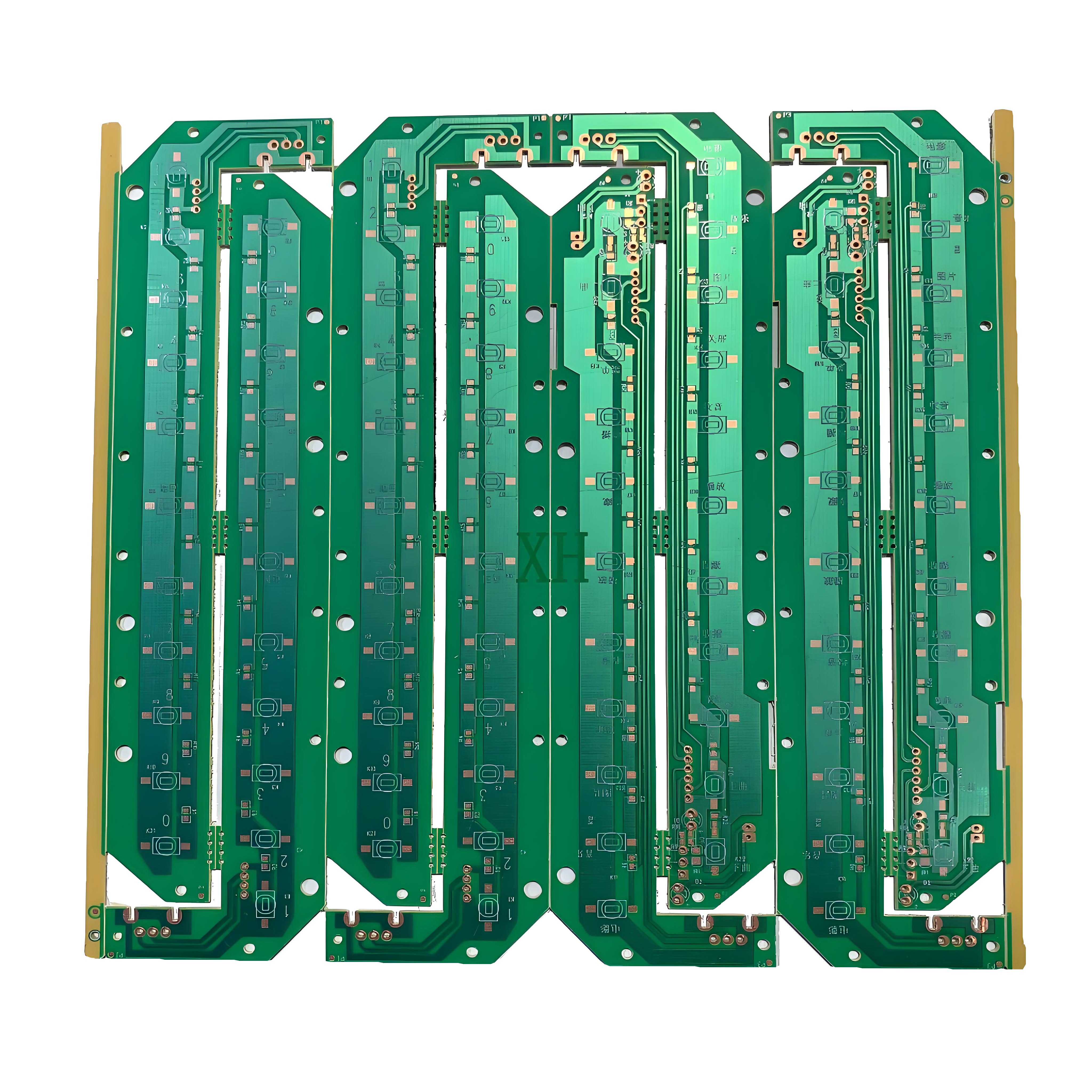
Classifications of PCB Manufacturing

specific applications and industries. Below are some of the most widely recognized PCB classifications:

By Type:

  • Rigid PCB
  • Flex PCB
  • Rigid-Flex PCB
  • HDI PCB
  • Aluminum PCB
  • Multilayer PCB
  • Microwave & RF PCB
  • Metal Core PCB
  • Custom PCB
  • Gold Finger PCB
  • Impedance Control PCB
  • Bare PCB

By Material:

  • FR4 PCB
  • Rogers PCB
  • Ceramic PCB
  • Polyimide PCB
  • Semiflex PCB
  • Isola PCB
  • Teflon PCB
  • Alumina PCB
  • High Tg PCB
  • Halogen-Free PCB
  • Copper-Based PCB
  • Taconic PCB
  • Low Loss PCB

By Feature:

  • Heavy Copper PCB
  • Blind and Buried Vias
  • Microvia PCB
  • VIPPO PCB
  • High-Frequency PCB
  • High-Speed PCB
  • Quick Turn PCB
  • Single-Sided PCB
  • Double-Sided PCB
  • 4-Layer PCB
  • 6-Layer PCB
  • IC Substrate PCB
  • Embedded PCB

By Application:

  • Power PCB
  • LED PCB
  • Inverter PCB
  • Control PCB
  • Sensor PCB
  • Amplifier PCB
  • Radar PCB
  • Medical PCB
  • Automotive PCB
  • Capacitive PCB
  • HVAC Circuit Board
  • UPS Circuit Board
  • Industrial PCB

With decades of development, PCB manufacturing has become integral to countless electronic products across diverse industries. Whether you need a basic single-layer PCB or a complex multilayer HDI board, understanding the history and classifications of PCB manufacturing can help you make informed decisions for your electronic designs.

PCB Manufacturing Steps: A Comprehensive Overview

PCB manufacturing is a detailed and intricate process, involving numerous steps to create both single/double-layer and multilayer PCBs. Here’s a brief introduction to the key steps involved in the production of these circuit boards:

Single/Double Layer PCB Manufacturing Process:

  1. Material Sheet Cutting: The process begins with cutting the base material to the required size.
  2. Drilling: Holes are drilled for components and interconnections.
  3. PTH & Copper Plating: Plated through-holes (PTH) and copper plating ensure connectivity between layers.
  4. Dry Film and Exposure: A dry film is applied and exposed to define the circuit pattern.
  5. Copper Etching: Unwanted copper is etched away, leaving the desired circuit paths.
  6. Copper Trace AOI: Automated Optical Inspection (AOI) checks for defects in copper traces.
  7. Quality Inspection: A thorough inspection is conducted to ensure quality.
  8. Solder Mask Printing: Solder mask is applied to protect the circuit.
  9. Components Marks Printing: Component identifiers are printed onto the board.
  10. Surface Treatment: Surface finishes are applied for protection and reliability.
  11. Outline Profiling: The PCB is cut to its final shape using CNC routing, v-cut, or punching.
  12. E-Testing: Electrical testing ensures the board functions as intended.
  13. Quality Checking: Final quality checks are conducted.
  14. Packaging: The PCBs are carefully packaged for shipment.

Multilayer PCB Manufacturing Process:

  1. Inner Layer Board Cutting: Base materials for inner layers are cut to size.
  2. Inner Layer Dry Film and Exposure: Similar to single/double layers, but applied to inner layers.
  3. Inner Layer Etching: Etching is done to form inner layer circuits.
  4. Inner Layer AOI: AOI inspects the inner layers for defects.
  5. Black Oxide: Inner layers undergo black oxide treatment for better adhesion.
  6. Layup and Lamination: Layers are stacked and laminated under heat and pressure.
  7. Board Cutting: The laminated board is cut to size.
  8. Drilling: Holes are drilled through the entire multilayer stack.
  9. PTH and Copper Plating: Plated through-holes are created, and copper is plated to form interconnections.
  10. Dry Film and Exposure: Outer layers are processed with dry film and exposure.
  11. Copper Etching: Copper is etched to form outer layer circuits.
  12. Outer Layer AOI: AOI checks the outer layers for defects.
  13. Solder Mask Printing: Solder mask is applied to the outer layers.
  14. Components Marks Printing: Components identifiers are printed on the outer layers.
  15. Surface Treatment: Surface finishes are applied to protect the outer layers.
  16. Outline Profiling: The final shape of the PCB is formed.
  17. E-Testing: Electrical testing verifies the functionality of the multilayer board.
  18. Packaging: The finished PCBs are carefully packaged for delivery.

Standards Used in PCB Manufacturing

The PCB manufacturing process adheres to various standards, with IPC standards being the most widely recognized. IPC, the global association for the electronics industry, sets standards for PCB manufacturing, ensuring quality and consistency.

IPC Standards for PCB Manufacturing:

  • PCB Acceptance Standards: IPC-A-600, IPC-6012, and more ensure that PCB quality meets specified classes.
  • Surface Finish Standards: Standards like IPC-4552 (ENIG) and IPC-4553 (Immersion Silver) define acceptable surface finishes.
  • PCB Laminates Specifications: IPC-4101 for rigid materials and IPC-4202 for flexible materials guide material selection.
  • Base Copper Foil Specifications: IPC-4562 and others define copper foil requirements.

Factors Influencing PCB Manufacturing Costs

PCB manufacturing costs vary depending on several factors, including:

  • Base Material Types: Different materials, such as FR4 or high-frequency laminates, have different price points.
  • PCB Dimensions: Larger PCBs require more materials, increasing costs.
  • Layer Counts: More layers involve more complex processes and higher costs.
  • Copper Thickness: Thicker copper layers add to the overall cost.
  • PCB Thickness: Both ultra-thin and very thick PCBs can be more expensive to produce.
  • Layup Structure: Special structures can add extra costs.
  • Blind/Buried Vias: Advanced via technologies increase manufacturing complexity and costs.
  • Surface Finishes: Different finishes, such as ENIG or hard gold plating, vary in cost.
  • Special Requirements: Features like impedance control, back drilling, or countersink holes can also affect pricing.

Choosing a Reliable PCB Manufacturing Supplier

When selecting a PCB manufacturing supplier, it’s crucial to consider factors such as ISO9001 and UL certifications, the company’s experience, focus on quality, and customer service. At LEAPPCB, we are ISO9001:2015 certified and UL listed, making us one of the most reliable PCB manufacturers in China.

The Current Landscape of PCB Manufacturing

Over the past century, PCB manufacturing technology has evolved significantly, becoming increasingly advanced and essential to the electronics industry. In this article, we explore the current state of PCB manufacturing, including the leading countries and regions, top manufacturers, and key applications in the industry.

Key Countries and Regions for PCB Manufacturing

From 2015 to 2021, the majority of the top 100 PCB manufacturing companies were based in Asia, particularly in Mainland China, Taiwan, Japan, and South Korea. Together, these regions account for approximately 93% of the global PCB industry’s total revenue.

  • Taiwan: Leading the market with 35% of global PCB production in 2021.
  • Mainland China: Contributing 28% of the global production, with steady growth.
  • Japan: Holding 18% of the market share.
  • South Korea: Accounting for 12% of global PCB production.
  • Other Regions: The remaining 7% of PCBs are produced in other countries around the world.

Among these, China’s PCB manufacturing sector has been experiencing consistent growth, solidifying its position as a global leader.

Main Applications of PCB Manufacturing

PCBs are indispensable in virtually every electronic device. The primary applications of PCB manufacturing include:

  • Communication Industry: Enabling the connectivity of modern communication devices.
  • Computer Industry: Integral to the function of computers and related hardware.
  • Industrial Control: Used in automation and control systems.
  • Medical Devices: Supporting critical functions in medical technology.
  • Automotive Electronics: Essential for vehicle control systems and infotainment.
  • Consumer Electronics: Found in everyday gadgets like smartphones, TVs, and more.

With the rapid development of technologies like 5G, the Internet of Things (IoT), cloud computing, and robotics, PCB manufacturing for these sectors is expected to grow rapidly.

The Future of PCB Manufacturing

PCBs are the foundation of electronic devices, crucial for integrating electronic components and enabling their functions. As technology continues to advance, PCB manufacturing is set to remain irreplaceable, with significant growth anticipated in the coming years.

  • Growth Projections: The global PCB industry saw a 20% increase in 2021, reaching an $80 billion annual turnover. This growth is expected to continue, with a projected 5% annual increase from 2022 to 2026, potentially exceeding $100 billion by 2026. China’s PCB manufacturing sector is expected to experience even greater growth.

  • High-Tech PCBs on the Rise: The demand for high-tech circuit boards, such as rigid-flex PCBs, HDI PCBs, and IC substrate PCBs, is expected to grow at an accelerated pace. This trend will require PCB manufacturers to invest in advanced equipment and technology to keep up with industry demands.

  • China’s Role: Leveraging its mature industrial chain and extensive customer base, China is poised to remain the dominant player in global PCB manufacturing. The country’s growth rate in this sector is likely to outpace the global average, contributing significantly to the advancement of the global electronics industry.

As the electronics industry continues to evolve with the expansion of 5G networks, artificial intelligence (AI), wearable technology, big data, new energy vehicles, Industry 4.0, and IoT, the importance of PCB manufacturing will only increase, driving innovation and growth worldwide.

Get Your Free Instant Quote Today!

Leap Electronic is your trusted partner and one-stop shop for PCB fabrication, component sourcing, PCB assembly, and electronic manufacturing. With over 16 years of expertise, we proudly serve over 1000 customers worldwide, delivering top-quality PCBs at competitive prices. Our ISO9001:2015 certification and UL listing ensure that all our products meet the highest industry standards. Every PCB is 100% E-tested and inspected using AOI and X-RAY, guaranteeing unparalleled reliability and performance.

Don’t wait – get an instant quote from our sales team today and experience the Leap Electronic difference. We’ll handle the rest!

Everything You Need to Know About Custom PCBs

Absolutely “Yes.” All PCBs are manufactured in strict compliance with IPC-A-600 Class 2 and 3 standards, UL standards, customer specifications, ISO9001:2015, and RoHS standards, ensuring the highest quality.

To receive a detailed quote for PCB manufacturing, please provide the following information:

  • PCB or Gerber files
  • Board thickness
  • Number of layers
  • Solder mask color
  • Silkscreen color
  • Surface finish requirements
  • Whether vias are covered with solder mask
  • Copper foil thickness
  • Quantity needed
  • Any other special requirements

For any inquiries, please feel free to reach out via email or phone. You can find our contact details on our official website: Contact Us. We look forward to assisting you.

If you experience any issues during PCB manufacturing, simply contact our sales team via email or phone. Our dedicated team is here to help resolve any concerns promptly.

IPC Class-III represents the highest standards for PCBs, essential for products requiring high reliability, such as those in automotive, military, aerospace, and marine industries. Class-III ensures continuous and dependable performance.

Yes, you can cancel your order. If cancellation occurs before production begins, it’s free of charge. However, if production has already started, the customer will be liable for associated costs as per our terms and conditions.

LEAPPCB accepts various payment methods:

  • Wire transfer to our bank
  • PayPal
  • Payoneer
  • Other methods can be discussed based on your needs

Lead time for PCB manufacturing starts from the date your order is placed.

We specialize in manufacturing a wide range of PCB types, including:

  • Rigid PCBs
  • Flexible PCBs
  • Rigid-Flex PCBs
  • HDI PCBs
  • Aluminum and Copper Base PCBs
  • High-Frequency and High-Speed PCBs
  • IC Substrate PCBs
  • And more specialized boards

Our PCBs are manufactured in Shenzhen, China—a global hub for technology and innovation. Shenzhen offers a robust industrial cluster, state-of-the-art manufacturing systems, and extensive resources, enabling us to provide top-quality products and services worldwide.

We proudly serve customers globally, with a focus on Europe, the United States, Canada, Australia, and other regions.

If you don’t have digital files for your PCB design, you can send us the physical board. We’ll copy and fabricate it according to your specifications.

Our PCB manufacturing capabilities include boards ranging from 0.1×0.1 inches to 21×59 inches. However, as our capabilities expand, we encourage you to contact our sales team for the most up-to-date information.

Our rigorous testing policy includes:

  • Electrical Open and Short Testing
  • Automated Optical Inspection (AOI)
  • Visual Inspection
  • Dimensional Inspection
  • Solderability, Thermal, and Peel Tests
  • Impedance and Ionic Contamination Tests
  • IPC-A-600 Class 2 and 3 Inspections

LEAPPCB holds several quality certifications, including:

  • ISO 9001:2015
  • ISO 13485:2016
  • ISO 14001:2015
  • UL E358677
  • IPC-A-600 Class 2 and 3

To track your order, communicate with our sales staff. They will provide you with timely updates and, after shipping, will send you the tracking number for your products.

We maintain budget efficiency by:

  1. Controlling raw material costs
  2. Reducing material and energy consumption while increasing productivity
  3. Maximizing facility utilization and shortening production cycles
  4. Eliminating waste in all forms

No, we do not have a minimum order quantity for PCB manufacturing. LEAPPCB focuses on low-to-medium volume PCBA services, along with prototyping and mass production.

Yes, all PCB manufacturing services come with a warranty. Specific terms are outlined in our agreements.

We may provide free samples under certain conditions. For details, please contact our sales team.

To get a quick quote, contact our sales team via email or phone. You can find their details on our Contact Us page. Typically, quotes are provided within one day, with some as fast as within an hour.

Break-away tabs are essential for aiding the assembly process in highly automated SMT production lines. They also assist in proper alignment during testing and help with the detection of board placement by SMT sensors.

The most critical factors in professional PCB manufacturing are:

  • An experienced engineering team
  • Skilled production workers
  • Advanced equipment
  • Effective management practices

China’s PCB manufacturing industry has grown rapidly, offering a wide range of high-quality, competitively priced PCBs, including standard FR-4, HDI, and rigid-flex PCBs. Leveraging China’s technological advancements and mature industry chain can greatly benefit your PCB needs.

China First 7-Day Delivery Headset Factory​, Free Samples Available.

Ask For A Quick Quote

We will contact you within 1 working day, please pay attention to the email with the suffix “@techpinn.com”