PCB Via Plugging
Professional Insights on PCB Via Plugging
Why is PCB Via Plugging Important?
- Enhanced Reliability: Plugging vias helps protect them from environmental contaminants like moisture and dust, which can lead to corrosion and failure over time.
- Improved Signal Integrity: By filling or covering vias, we can reduce signal loss and noise, ensuring better performance in high-frequency applications.
- Preventing Solder Wicking: Plugged vias prevent solder from flowing through the via during the assembly process, which is crucial in ensuring that solder joints are strong and reliable.
- Thermal Management: In some cases, plugging vias can help in better heat dissipation, which is essential for maintaining the thermal stability of the PCB.
What is PCB Via Plugging?

PCB via plugging is a specialized process where the vias—small holes that allow electrical connections between different layers of a printed circuit board (PCB)—are filled or covered. This technique is essential for improving the performance, reliability, and longevity of PCBs, particularly in complex designs where space is at a premium or where the board operates in challenging environments.
Request Your Free Quote Today!
Common Types of Via Plugging in PCBs
At LEAPPCB, we offer several types of via plugging to suit different PCB requirements, including conductive via plugs, non-conductive via plugs, and via plating shut by copper.
Via Tenting with LPI Solder Mask
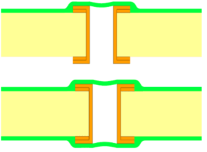
- Description: Plated through vias are covered with an LPI solder mask on one or both sides of the PCB during the solder mask printing process.
- Advantages:
- Cost-effective
- Helps prevent solder leakage during SMT
- Protects against dust and liquid ingress
- Disadvantages:
- Vias may not be fully covered
- Not suitable for BGA areas
- Best for vias under 0.3mm, with a maximum of 0.5mm
Via Plugging with Solder Mask
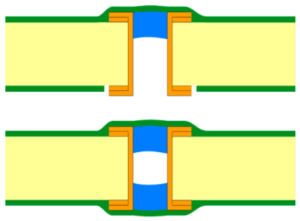
- Description: An additional process where vias are specifically plugged with solder mask, either on one or both sides of the PCB.
- Advantages:
- Minimal additional cost
- Nearly 100% via coverage
- Effective in preventing solder leakage and contamination
- Disadvantages:
- Not ideal for BGA areas
Non-Conductive Via Plugging

- Description: Vias are filled with non-conductive material, typically epoxy, ensuring complete coverage. This method is often used for BGA areas where space constraints require direct via drilling into BGA pads.
- Advantages:
- Completely prevents solder leakage and contamination
- High stability and reliability
- Disadvantages:
- Additional cost
- Requires experienced manufacturing and specialized equipment
Conductive Via Plugging

- Description: Vias are filled with conductive material to ensure full plugging and enhanced thermal conductivity.
- Advantages:
- Excellent for heat dissipation
- Improved current carrying capacity
- Completely prevents solder leakage and contamination
- High stability and reliability
- Disadvantages:
- Higher cost
- Requires careful material selection to prevent via fracture
Via Plated Shut by Copper

- Description: Instead of filling the vias with material, the vias are fully plated shut with copper. Due to the complexity and cost, this method is less commonly used.
- Advantages:
- Superior heat dissipation and current carrying capacity
- Fully sealed to prevent solder leakage and contamination
- Excellent stability and reliability
- Disadvantages:
- Very high cost
- Limited by via size and copper thickness constraints
Each via plugging method has its specific advantages and is chosen based on the design requirements, reliability needs, and cost considerations of the PCB.
Overview of IPC 4761: Guide for PCB Via Protection Types
In the PCB manufacturing process, we adhere to IPC 4761 standards for via protection. Below is an explanation of the various types of via protection as outlined in IPC 4761, the definitive guide for the protection of printed board via structures.
| IPC-4761 Type | Description | Material Used | Reliability | Cost | Availability |
|---|---|---|---|---|---|
| Type I-A | Tented Vias – Single-Sided | Dry Film | Low | Low | No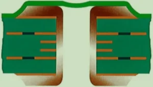 |
| Type I-B | Tented Vias – Double-Sided | Dry Film | Low | Low | No |
| Type II-A | Tented and Covered Vias – Single-Sided | Dry Film/LPI Solder Mask | Medium | Low | Yes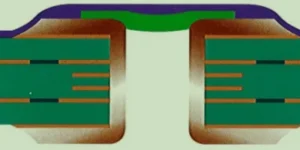 |
| Type II-B | Tented and Covered Vias – Double-Sided | Dry Film/LPI Solder Mask | Medium | Low | Yes |
| Type III-A | Plugged Vias – Single-Sided | LPI Solder Mask or Resin | Medium | Low | Yes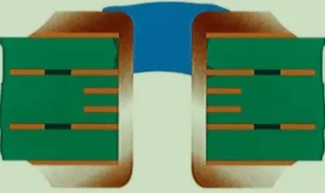 |
| Type III-B | Plugged Vias – Double-Sided | LPI Solder Mask or Resin | Medium | Low | Yes |
| Type IV-A | Plugged and Covered Vias – Single-Sided | LPI Solder Mask or Epoxy | Medium | Low | Yes |
| Type IV-B | Plugged and Covered Vias – Double-Sided | LPI Solder Mask or Epoxy | Medium | Low | Yes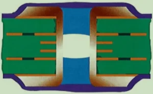 |
| Type V | Filled Vias (Fully Plugged) | Conductive or Non-Conductive Material | High | Medium | Yes |
| Type VI-A | Filled and Covered Vias – Single-Sided | Conductive or Non-Conductive Material + LPI Solder Mask | High | Medium | Yes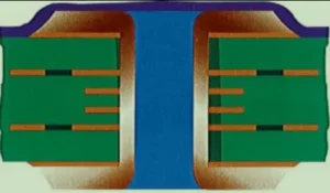 |
| Type VI-B | Filled and Covered Vias – Double-Sided | Conductive or Non-Conductive Material + LPI Solder Mask | High | Medium | Yes |
| Type VII | Filled and Capped by Copper | Conductive or Non-Conductive Material + Copper Plating | High | High | Yes |
These classifications help ensure the proper protection and reliability of vias, tailored to specific design and manufacturing needs.
Get Your Free Instant Quote Today!
Leap Electronic is your trusted partner and one-stop shop for PCB fabrication, component sourcing, PCB assembly, and electronic manufacturing. With over 16 years of expertise, we proudly serve over 1000 customers worldwide, delivering top-quality PCBs at competitive prices. Our ISO9001:2015 certification and UL listing ensure that all our products meet the highest industry standards. Every PCB is 100% E-tested and inspected using AOI and X-RAY, guaranteeing unparalleled reliability and performance.
Don’t wait – get an instant quote from our sales team today and experience the Leap Electronic difference. We’ll handle the rest!
