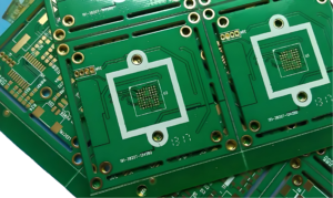
Rigid PCBs
Superior Rigid PCBs at Competitive Prices
- Mass production from 1-40 layers, with up to 100 layers for prototypes.
- Expertise in FR4, high-speed, microwave & RF, metal core, ceramic, and PTFE materials.
- Proficiency in blind & buried vias, stacked & staggered vias, and any-layer HDI.
- Conductive and non-conductive via plugging for enhanced performance.
- Back drilling, backplane solutions, embedded devices, and IC substrates.
- ISO 9001:2015 certified and UL listed for assured quality and safety.
In every corner of the world, electronic devices enhance our daily lives by simplifying complex tasks. Common household appliances like vacuum cleaners, washing machines, refrigerators, and televisions exemplify this convenience. Today, many of these devices are considered “smart,” capable of operating autonomously with exceptional efficiency and effectiveness. At the heart of these innovations are rigid printed circuit boards (PCBs), which power everything from basic functions to advanced operations. Despite the advent of various PCB types, rigid PCBs remain a cornerstone in modern manufacturing. Join us as we delve into the world of rigid printed circuit boards and explore their pivotal role in today’s technology.
Request Your Free Quote Today!
Understanding Rigid PCBs
A rigid PCB, or printed circuit board, is constructed from a solid substrate material that remains inflexible and unchangeable once manufactured. As a traditional and widely used type of PCB, rigid PCBs are prevalent in automotive, commercial, and industrial applications. The most commonly used and commercially available rigid PCB substrate is FR4, a flame-retardant epoxy woven fiberglass. FR4 is renowned for its excellent hardness, dielectric properties, and thermal performance. The choice of rigid PCB laminate material varies based on the application, with some requiring materials featuring a low coefficient of thermal expansion or specific dielectric constants.
Rigid PCBs are typically composed of three primary layers: 
- Insulating Substrate: Often FR4, this layer provides the board’s structural integrity and insulation.
- Copper Layer: This conductive layer is etched to form the circuit pathways. Thicker copper layers offer better current-carrying capacity.
- Photoresist Layer: This protective layer shields the copper pathways.
Rigid PCBs can be categorized based on the number of layers they contain:
- Single-Sided: Featuring circuitry on one side of the board.
- Double-Sided: With circuitry on both sides, allowing for more complex designs.
- Multi-Layered: Consisting of multiple layers, these boards support higher functionality and require more intricate fabrication processes.
Rigid PCBs are integral to the functioning of countless electronic devices, providing a stable and reliable platform for complex circuitry. Their robust construction and versatile applications make them a cornerstone of modern electronic design and manufacturing.
Discover the Advantages of Rigid PCBs
Rigid printed circuit boards (PCBs) offer numerous benefits, making them a preferred choice in many applications. Here are the key advantages: 
Superior Mechanical Strength
Rigid PCBs are known for their robust mechanical structures, providing greater durability compared to flexible PCBs. Their resistance to expansion and deformation ensures long-lasting performance.
Enhanced Functionality
With the ability to support multiple layers and high connection density, rigid PCBs offer greater functionality and design flexibility. This makes them ideal for complex electronic systems.
Efficient Manufacturing
As one of the earliest PCB technologies, rigid PCBs benefit from well-established, efficient, and automated manufacturing processes. This maturity translates to cost-effective and reliable production.
High Reliability
Rigid PCBs are highly reliable, making them essential for applications where stability and durability are critical. Their structural rigidity ensures they maintain integrity under various conditions.
Step-by-Step Guide to Fabricating Rigid PCBs
Rigid PCBs are crucial in numerous electronic devices, and their fabrication involves several precise steps to ensure quality and reliability. Here’s a detailed guide to the fabrication process:
1. Schematic Design and PCB Layout
Start by creating a schematic diagram using computer-aided design (CAD) software. This schematic maps out each component and connection on the PCB. Next, develop the PCB layout, which visualizes the final physical appearance of the rigid PCB.
2. Lamination
Lamination involves bonding prepreg sheets with copper foil layers under heat and pressure. The prepreg contains uncured resin, which becomes viscous and then solidifies during lamination. This process occurs in a controlled hot-pressing machine.
3. Photoresist Application
Apply a photoresist layer to protect the copper from oxidation. Positive photoresist is commonly used, where exposed areas become soluble under UV light and can be developed with chemicals like sodium hydroxide.
4. Etching
Etch out the unwanted copper using etchants such as ferric chloride or ammonium chloride. This step removes excess copper, leaving the desired circuit pattern. Ensure consistent etching quality by controlling the etch rate and bath concentration.
5. Drilling
Use computer-programmable drilling machines to create holes and vias. High-precision drills with diamond or tungsten carbide tips are used, especially for miniaturized components. Optimize drill speed and force for accuracy.
6. Solder Masking
Apply a solder mask to protect the PCB’s conductive and insulating surfaces. This layer is applied using Liquid Photo-imageable Solder Masks (LPSM) and cured with UV light, or through epoxy liquids that are thermally cured.
7. Surface Finish
To prevent copper oxidation, apply a surface finish to exposed pads. Options include Hot Air Solder Leveling (HASL) and Electroless Nickel Immersion Gold (ENIG), both ensuring effective soldering and connectivity.
8. Silkscreen
Silkscreening adds vital information to the PCB, such as component codes, pin locators, and company logos. This can be done using stencils and squeegees or Liquid Photo Imaging (LPI) for high-density PCBs, using light-sensitive ink that is developed and cured.
By following these meticulous steps, you can fabricate high-quality rigid PCBs that meet the demands of various electronic applications. Ensuring precision at each stage guarantees a reliable and efficient final product.
Applications of Rigid PCBs: Versatile and Reliable
Rigid PCBs are essential components in numerous industries due to their durability and dependable performance. Key applications include:
- Consumer Electronics: Computer motherboards, storage devices, and mobile phones.
- Communication Technologies: Satellite systems, radios, and antennas.
- Automotive Industry: Infotainment systems and control systems.
- Medical Equipment: Diagnostic devices and life-saving machines.
- Industrial Electronics: Control systems and instrumentation.
- Military Applications: Defense electronics and communication devices.
Rigid PCBs are crucial for modern technology, driving innovation and ensuring reliability across various sectors.
Why Choose LEAPPCB as Your Rigid PCB Partner?
Unmatched Capabilities
LEAPPCB specializes in providing a comprehensive range of rigid PCB solutions, accommodating various materials, layer counts, copper thicknesses, surface finishes, and technologies. Whether you require a straightforward one-layer PCB or a complex 100-layer HDI PCB with intricate vias and fine lines, we have the expertise to fulfill all your needs.
Competitive Pricing
We offer competitive pricing with flexible options tailored to your requirements. Share your technical specifications with us, and we will promptly provide you with a detailed quotation.
Superior Quality
Quality is at the heart of everything we do at LEAPPCB. Our commitment to delivering high-quality rigid PCBs is unwavering, driven by a zero-defect mindset and a culture of continuous improvement. Our production processes adhere to stringent quality management standards, including ISO9001, ISO13485, and TS16949.
Exceptional Customer Service
At LEAPPCB, we believe that open communication and collaboration are the keys to a successful partnership. We treat our customers as partners, aligning our goals with yours to ensure your success. We prioritize your needs and requests, delivering on our commitments every time.
Fast and Reliable Delivery
We are known for our reliability in meeting delivery deadlines. LEAPPCB offers fast turnaround times and expedited options to ensure your projects stay on track. Our adherence to delivery commitments is a testament to our dedication to your success.
Choose LEAPPCB for your rigid PCB needs and experience unparalleled service, quality, and expertise. Contact us today to discuss your project requirements!
Get Your Free Instant Quote Today!
Leap Electronic is your trusted partner and one-stop shop for PCB fabrication, component sourcing, PCB assembly, and electronic manufacturing. With over 16 years of expertise, we proudly serve over 1000 customers worldwide, delivering top-quality PCBs at competitive prices. Our ISO9001:2015 certification and UL listing ensure that all our products meet the highest industry standards. Every PCB is 100% E-tested and inspected using AOI and X-RAY, guaranteeing unparalleled reliability and performance.
Don’t wait – get an instant quote from our sales team today and experience the Leap Electronic difference. We’ll handle the rest!
Frequently Asked Questions about Rigid PCBs
- FR4 Material: Standard for many applications.
- High Signal Speed Materials: Optimized for fast data transfer.
- High-Speed FR4 Substrate: Available for both 1GHz and 10GHz frequencies.
- Low Df Ceramic Material: Excellent performance at 10GHz.
- PTFE and Reinforced PTFE: Known for high-temperature resistance.
Rigid PCBs are crafted using several advanced techniques, including:
- Lamination
- Drilling
- Copper Plating
- Copper Etching
- Solder Mask Application
- Surface Finishing
- Component Silkscreening
- Depanelization
- Comprehensive Testing
To ensure quality and reliability, rigid PCBs are subjected to various tests, such as:
- Electrical Tests for Opens and Shorts
- Automated Optical Inspection (AOI)
- TDR Impedance Testing
- Hi-Potential Testing
- Visual Defects Inspection
- Solderability Testing
- Thermal Testing
- Tape Test
- Peel Test
- Ionic Contamination Testing
Production times vary depending on the order size:
- Quick Turn: 1-5 days.
- Prototypes & Small Series: 1-2 weeks.
- Mass Production: 2-4 weeks.
- Materials: Rigid PCBs use FR4, ceramic, metal core, PTFE, etc. Flex PCBs use polyimide (PI), PET, Kapton.
- Flexibility: Rigid PCBs cannot bend, while flex PCBs are highly bendable.
- Applications: Rigid PCBs are used in stationary devices, whereas flex PCBs are ideal for devices with moving parts like cameras and mobile phones.
Several factors influence the cost:
- Type of base material
- Number of layers
- Copper thickness
- PCB thickness
- Layup structure
- Blind/Buried vias
- Surface finishes
- Special technologies or requirements
- High Dimensional Stability
- High Reliability
- Cost-Effective
- Lack of Flexibility: Not suitable for applications requiring bending.
- Heavier Weight: Not ideal for lightweight, portable, or wearable devices.
Rigid PCBs, especially those made from FR4 and aluminum, are the most cost-effective option compared to flexible or rigid-flex PCBs, making them ideal for consumer products requiring low-cost solutions.
Rigid-flex PCBs combine the properties of both rigid and flexible circuit boards, offering versatility in design and application.
